
By Franky Nguyen, AVF Decolletage
Introduction
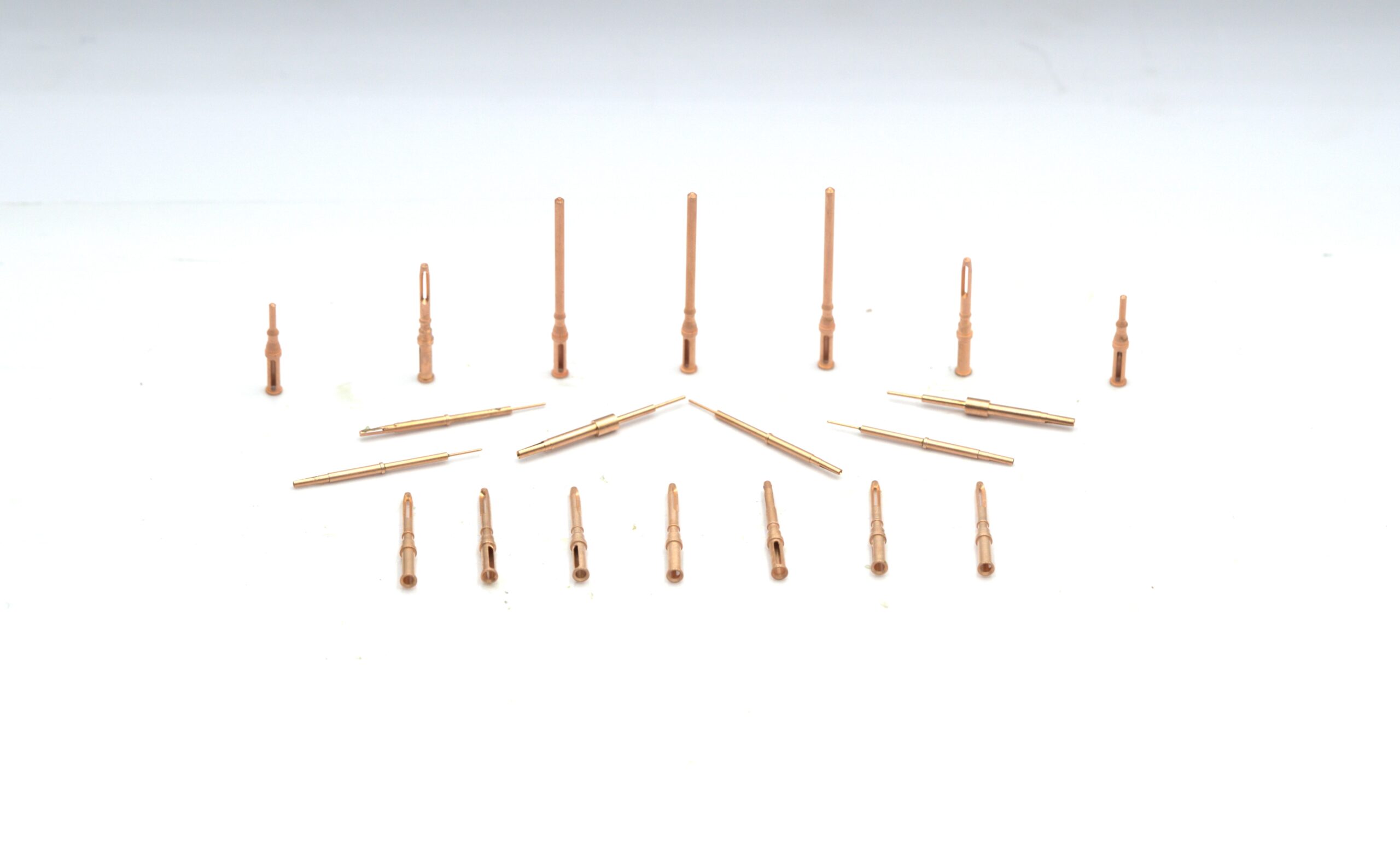
Test Probe Manufacturing is entering a new era. As electronics get smaller, faster, and smarter, the humble test probe must evolve to keep pace. Future generations of test probes are being engineered for miniaturization, high-frequency performance, automation compatibility, and sustainability.
At AVF Decolletage, we’re investing in new Swiss CNC machining technologies, next-generation materials, and intelligent inspection systems to support the industries of tomorrow. In this article, we explore how innovation is reshaping test probe design and what it means for manufacturers, engineers, and global OEMs.
1. Miniaturization — Testing in Microscopic Spaces
One of the biggest challenges in modern test probe manufacturing is fitting into increasingly compact devices. From microchips to wearable medical sensors, space is at a premium.
To meet this demand, manufacturers are now producing ultra-micro test probes with diameters below 0.25 mm. Achieving such precision requires:
-
Advanced Swiss CNC micro-machining with multi-axis control.
-
Non-deforming tips that maintain consistent contact pressure.
-
Gold-plated brass or beryllium copper (C17300) to ensure conductivity at tiny scales.
As a result, test probes are now enabling inspection of semiconductors, MEMS devices, and high-density PCBs that were once impossible to access.
Explore our Swiss CNC capabilities.
2. High-Frequency and High-Speed Testing
Future electronics operate at lightning speed — think 5G, radar systems, and high-speed computing. Test probes must handle these frequencies without signal loss or distortion.
Next-generation test probe manufacturing now focuses on:
-
Optimized geometry for reduced inductance and capacitance.
-
Low-resistance plating to improve signal flow.
-
Stable spring design to maintain constant contact under vibration.
By balancing mechanical performance and electrical integrity, future probes will enable accurate testing at gigahertz frequencies — a must for telecommunications and aerospace sectors.
3. Reliability Through Smart Materials
Tomorrow’s probes will not only be smaller but also stronger and longer-lasting. Material innovation is key to that transformation.
New trends include:
-
Composite alloys with higher fatigue resistance.
-
Hybrid coatings that combine gold’s conductivity with nickel’s durability.
-
Surface texturing to enhance wear resistance.
At AVF Decolletage, our R&D teams are testing alloys that deliver both conductivity and resilience — ensuring test probes can withstand millions of contact cycles without degradation.
See our material certifications.
4. Automation and Smart Manufacturing
The future of test probe manufacturing is not just about the probe — it’s also about how it’s made.
Smart factories are adopting AI-driven machining and quality control to improve consistency and reduce waste. AVF Decolletage has already implemented:
-
Automated CNC loading systems for continuous production.
-
Vision-based inspection to identify micron-level surface defects.
-
Data-driven quality tracking for traceability and predictive maintenance.
These technologies make production faster, more sustainable, and more cost-efficient — aligning with the demands of global electronics manufacturers.
Learn more about our quality system.
5. Sustainable Test Probe Manufacturing
Sustainability is becoming central to product design. The next wave of test probes will be made not only for durability but also for environmental responsibility.
AVF Decolletage is already taking steps toward greener production through:
-
Recycling brass and stainless steel scrap.
-
Reducing plating waste with optimized chemical use.
-
Investing in energy-efficient Swiss CNC machines.
As environmental regulations tighten, sustainability will no longer be optional — it will define how OEMs select their partners.
6. Customization and Modularity
The future will also bring a move toward modular test probe systems. Engineers will no longer rely on one-size-fits-all probes. Instead, they’ll assemble modular heads, springs, and barrels to suit specific test conditions.
AVF Decolletage’s engineering team is developing configurable probe assemblies that give customers flexibility in design and function — speeding up testing and reducing tooling costs.
Conclusion
The future of test probe manufacturing is built on innovation — smaller probes, faster testing, smarter materials, and sustainable production.
At AVF Decolletage, we’re proud to lead this transformation. With Swiss CNC precision, ISO-certified systems, and continuous R&D, we’re designing the next generation of probes that will power the electronics of tomorrow.
FAQ
Q1: What drives the future of test probe manufacturing?
Miniaturization, high-frequency testing, automation, and sustainability.
Q2: What is the smallest probe AVF Decolletage can produce?
We currently manufacture probes below 0.25 mm in diameter.
Q3: How does automation improve probe quality?
It enhances consistency, reduces defects, and increases production speed.
Q4: Are future probes recyclable?
Yes, brass and stainless steel probes are fully recyclable.
Q5: Why partner with AVF Decolletage?
Because we combine Swiss precision, innovation, and a proven quality system trusted by global OEMs.